Production Technologies
Thanks to collaboration with the most important national and international fab-lines, Optoi is able to design, develop and supply silicon devices using:
- the best sensing solutions with planar technology, which are valid for photodiodes, phototransistors and other state-of-the-art detectors;
- CMOS techniques, for the implementation of integrated electronics, usually used as support for sensors (ASIC);
- MEMS micromachining techniques, to create low consumption 3D sensing devices: for example, this is applicable to transducers used for acceleration, flow, pressure, etc.

Front end - silicon wafer production
Smart and innovative microsystems and hybrid systems can be achieved by combining the above-mentioned technologies, which are customised and intended to satisfy the performance required by the customer.
This is the case with optical fibre detectors, where not only the receiver (photodiode) must be developed but a high-speed, low-noise signal conditioning circuit (photoASIC) is also required, often built on the same chip.
This is also the case of photodiodes used in very high reliability space, military and industrial applications, where very reliable detectors, which are uniform and resistant to particularly harsh environments (radiation, strong thermal excursions, vibrations, etc.) must be developed.
The opportunity to collaborate with colleagues in the FBK research centre in Trento, operating a few kilometres away from the Optoi head offices, is of enormous value, where a production line runs with the microfabrication of photoreceivers and MEMS on 6” silicon wafers (150 mm). The qualified staff of researchers and technicians is able to co-design and subsequently produce a vast variety of microelectronic devices, using industrial quality standards that conform to ISO 9001 and to the aerospace industry standards.

Back end - microlectronic packaging
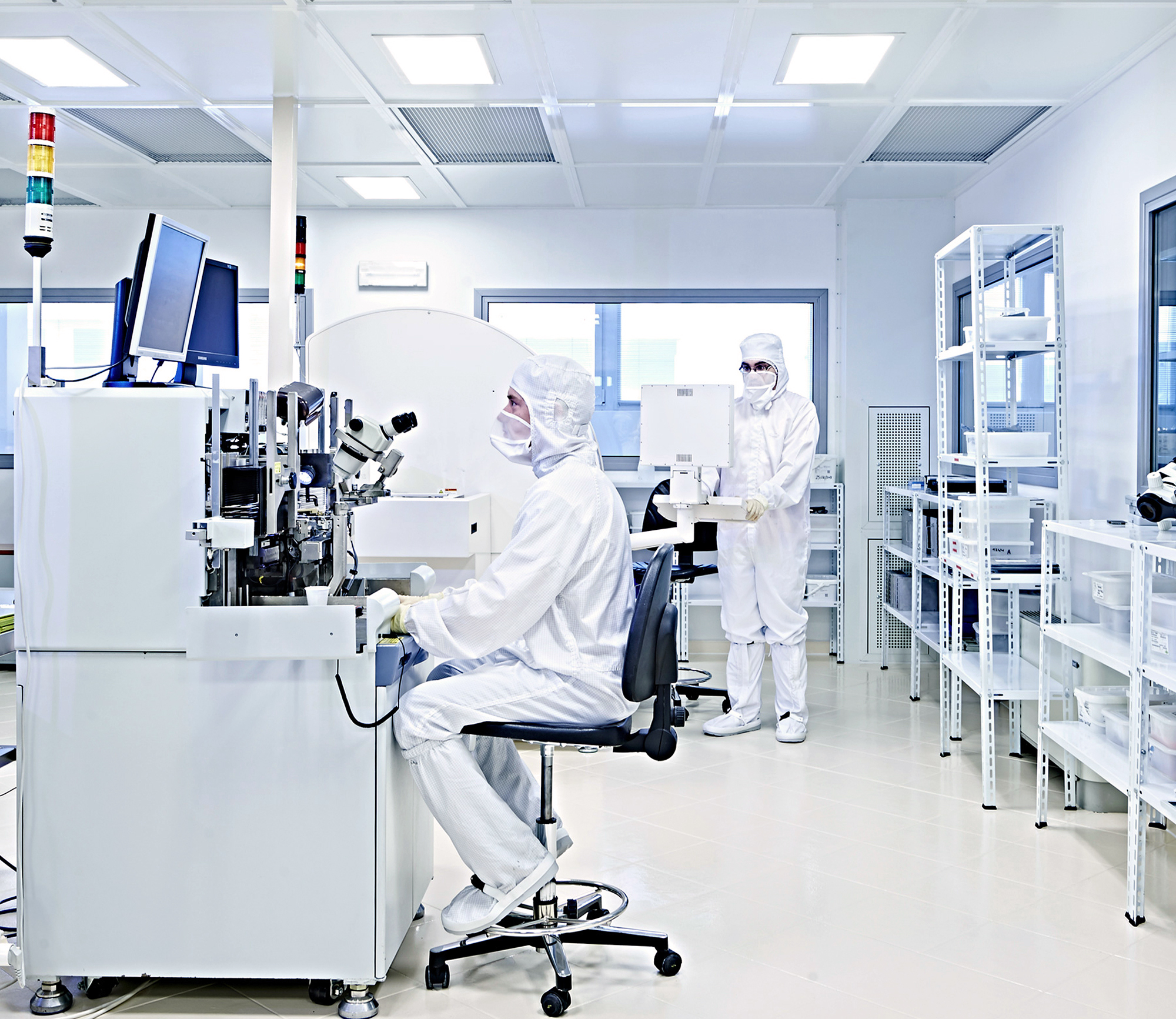
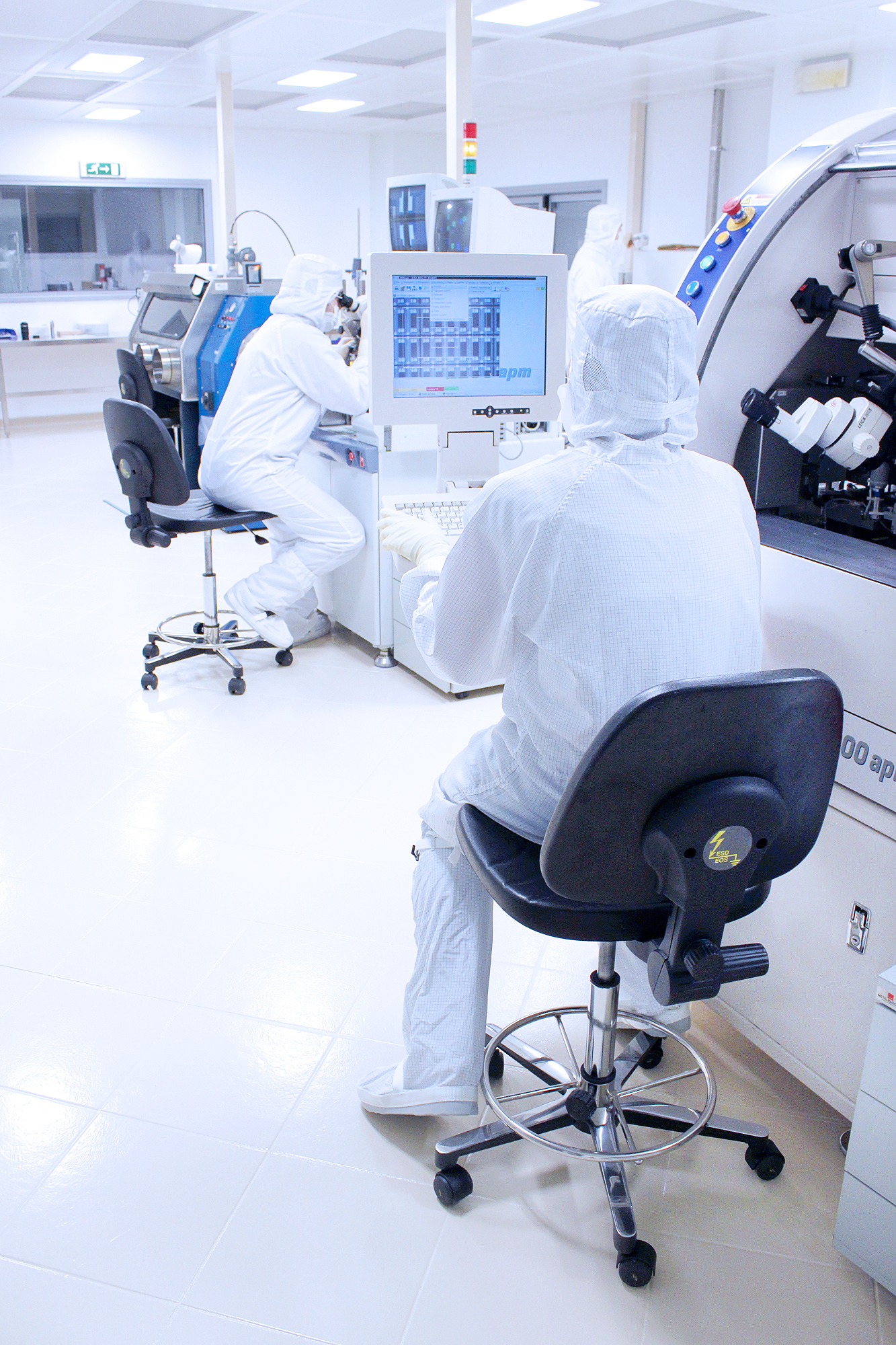
In particular, Optoi boasts great experience and expertise in the so-called back-end, which is a process implemented entirely in-house thanks to a class 1000 (ISO 6) cleanroom.
The back-end activity consists in creating the packaging for the microelectronic device and more specifically, positioning the dies in a suitable “container package” for soldering on the board.
Packaging requires specific skills in materials engineering, microelectronics engineering, telecommunications engineering and physics.
Aspects of electromagnetic compatibility, radio frequencies, optics, thermomechanics, reliability and robustness are on the agenda in the design and production of components.
Optoi uses its own automated lines to produce devices of the right quality with the right cost, and ranges from the production of components in large quantities at low cost (typical in the industrial sector), to the production of smaller batches with high technological value (typical in the aerospace sector).
Although Optoi has all the skills and interest to produce and sell complete components, company flexibility allows them to work even in partial service, creating for example, only some of the production stages for a customer, such as wafer cutting, precise depositing of filters or lenses, a chip on board on an already populated electronic board, volumetric embedding, etc.
Microelectronic automatic line packaging technologies:
- Wafer dicing and cleaning
- Die bonding
- Ultrasonic gold wire bonding
- Automated pressure/time and volumetric dispensing
- Hermetic projection welding
- Package/substrate level sawing
Main packaging solutions:
- Plastic SMD (Surface Mount Device)
- Metallic (TO-18, TO-46, TO-5, TO-8, etc.)
- Ceramic (CLCC, LTCC, etc.)
- COB (Chip On Board)
- CSP (Chip Scale Package)
- MCM (Multi Chip Module)
- Stack 3D (Module with 3D Stacked Multi Chip)
- Microsystems (for sensors and/or actuators and/or other integrated functions)
Key materials used:
- Semiconductors (wafers and dies: silicon, EPI, SOI, Gallium Arsenide, Germanium, etc.)
- Plastics (epoxy resins, silicone resins, polyurethane, UV)
- Metals (kovar, aluminum, steel, etc.)
- Ceramics (white alumina, glass, quartz, zirconia, black alumina, etc.)
- Composites (reinforced fibreglass, G200, FR4, Kapton, polyamide, Teflon, etc.).

SMT - electronic production and testing
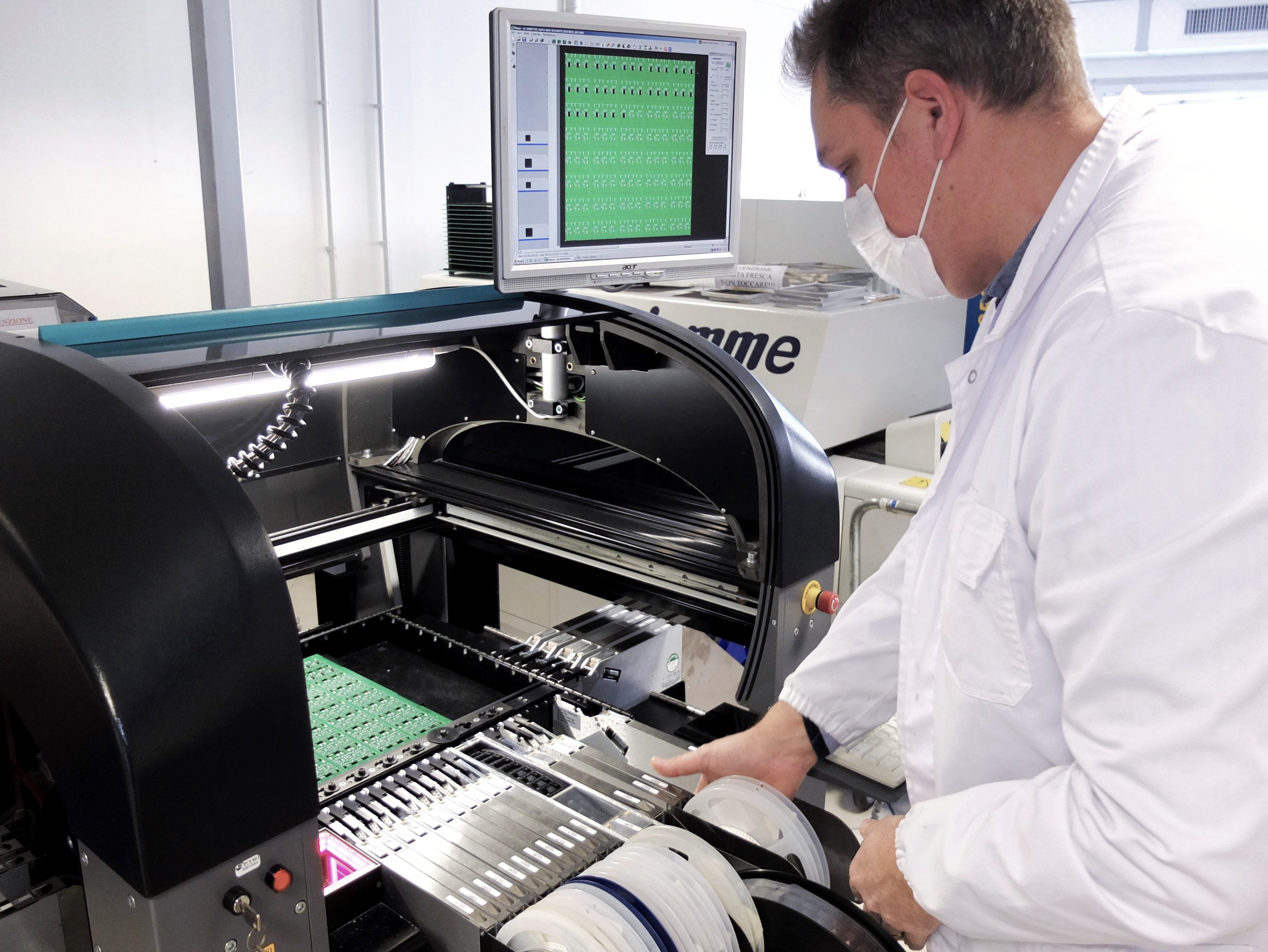
Optoi has a SMT assembly line consisting of:
Optoi has the means to perform on its premises operations such as the assembly of pin-thru-hole components, cabling and mechanical assembly on specifically equipped benches using qualified personnel.
Optoi also boasts application know-how as regards the resin reinforcement phase, both in the choice of resin suited to the product to be produced and in the setting and optimisation of the production process.
All of the electronic products are 100%-tested for electric and functional performance on dedicated test benches specifically designed and manufactured for each specific device.
- Screen printer
- Pick and Place
- 4-zone reflow oven.
Optoi has the means to perform on its premises operations such as the assembly of pin-thru-hole components, cabling and mechanical assembly on specifically equipped benches using qualified personnel.
Optoi also boasts application know-how as regards the resin reinforcement phase, both in the choice of resin suited to the product to be produced and in the setting and optimisation of the production process.
All of the electronic products are 100%-tested for electric and functional performance on dedicated test benches specifically designed and manufactured for each specific device.
Environmental simulation test chambers
For tests in a 0 to 100% humidity range and -40°C to +180°C temperature range
Test bench for electromagnetic compatibility measurements
Immunity test:
- IEC 61000-4-2 ESD
- IEC 61000-4-4 EFT
- IEC 61000-4-5 Surge